On September 4, Bloomberg reported that DeepSeek plans to deploy at least 160,000 Huawei Ascend 950DT accelerators in a gigawatt-scale data center it is building in Inner Mongolia, one of the largest known Huawei-chip clusters anywhere. The chips are for inference only; DeepSeek still trains on NVIDIA hardware it managed to keep. Fulfilling the order could take more than a year, because Huawei’s 950DT output in 2026 is capped in the low hundreds of thousands by component shortages (memory, of all things).
The same season, Jensen Huang said NVIDIA’s China revenue has dropped to “essentially zero” and that NVIDIA has “largely conceded” the market to Huawei. Whether that’s a full retreat or a temporary posture is genuinely unclear (Washington approved H200 sales to Chinese firms in December 2025, and Beijing made sure almost none were delivered), but the direction is not: the market share NVIDIA doesn’t have anymore is being filled by a chip that, eighteen months ago, did not exist.
The Ascend 950 is interesting precisely because of what it is not. It is not a TSMC-class chip built on a bleeding-edge EUV node; it can’t be, because SMIC has no EUV machines and can’t buy one. It is a chiplet package on a DUV-only 7nm-class process, wrapped in self-developed HBM, glued by a homegrown interconnect into systems of up to 8,192 chips, and fed by a software stack that now claims day-zero support for the most popular open model on Earth. This post takes it apart: the process, the architecture, the package, the system, and an honest look at what’s still missing.
How export controls became a design specification
The timeline matters, because each US restriction converted directly into a Huawei design decision:
| Date | Control | Consequence for Huawei |
|---|---|---|
| Oct 2022 | A100/H100-class export ban | Ascend 910 becomes stranded hardware |
| Oct 2023 | A800/H800 loopholes closed | No compliant NVIDIA parts above ~half H100 |
| 2024 | NVIDIA ships H20, built to comply | The “legal” chip becomes China’s default |
| Dec 2024 | HBM banned (ECCN 3A090.c: any stack >2 GB/s/mm² of bandwidth density) | Every production HBM stack qualifies: Huawei must build its own |
| Sep–Nov 2024 | TSMC dies found in 910B/910C teardowns; TSMC halts supply (~$500M penalty reported) | Stockpiled TSMC 7nm dies (~2.9M, per SemiAnalysis) become a dwindling asset |
| Apr 2025 | H20 license requirement | ~$4.5B NVIDIA write-off; China’s default chip gone |
| Aug 2025 | 15% China-revenue deal; H20 briefly returns | Sep 2025: Beijing’s CAC discourages NVIDIA purchases |
| Nov 2025 | B30A (Blackwell-class for China) blocked | The ceiling on legal NVIDIA silicon freezes |
| Dec 2025 – May 2026 | H200 approved; Beijing stalls deliveries, then formally bars big buyers | Huang: China revenue “essentially zero” |
Sources: BIS press releases, CSIS analysis, Tom’s Hardware’s Huawei teardown coverage, SemiAnalysis, Reuters, FT via China AI Dispatch.
The December 2024 HBM ban is the one most people undersell. HBM is where bandwidth lives, bandwidth is what inference runs on, and until that day every Chinese accelerator used Samsung or SK Hynix stacks. Cutting HBM off didn’t slow Huawei’s roadmap: it added a product line to it. The HiBL 1.0 and HiZQ 2.0 memory stacks on the Ascend 950 exist because the alternative was no memory at all.
By 2025 the strategy had stopped being “evade the controls” and become “build a parallel stack”: SMIC for silicon, HiSilicon for HBM, the Unified Bus for interconnect, CANN for software. The Ascend 950 is the first chip designed end-to-end inside that constraint set. That’s the lens for everything below.
SMIC N+3: a 7nm-class node without EUV, measured at last
The Ascend 950’s compute dies are widely reported to be made on SMIC’s N+3 process (analyst reporting: TrendForce, citing EE Times China and Eastmoney; Huawei itself only says “fully self-controlled manufacturing”). Whatever the fab assignment, N+3 is real and well-characterized now, because it ships in Huawei’s Kirin 9030 smartphone SoC, and two teardown firms have cut it open.
TechInsights confirmed in December 2025 that the Kirin 9030 is built on N+3, a “scaled extension” of SMIC’s 7nm N+2, and explicitly not a 5nm-class node. Then SemiAnalysis’s STEEL teardown in June 2026 put numbers on it, and the numbers are more interesting than the marketing:
| Metric | SMIC N+3 | TSMC N6 | Intel 18A (shipping) |
|---|---|---|---|
| Min metal pitch (M0) | 32.5 nm | ~40 nm | 36 nm |
| Transistor density | 113.4 MTr/mm² | 107.7 MTr/mm² | ~38% higher (normalized, HD library) |
| Patterning of critical layers | SAQP (M0, fin), SADP (M1/M2) | EUV | EUV |
| Transistor | FinFET, 2 fins (depominated) | FinFET | GAA RibbonFET |
| Backside power | No | No | Yes (PowerVia) |
| Lithography | DUV immersion only | EUV + DUV | EUV + DUV |
Cell height is 228 nm (5.7-track), with contact-over-active-gate and single diffusion breaks: aggressive DTCO, in other words, squeezing density out of design rules rather than lithography. The 32.5 nm M0 pitch is tighter than what Intel ships on 18A, and density edges past TSMC N6, a node that uses EUV.
Read those comparisons carefully, though. The pitch headline is one SemiAnalysis itself calls cherry-picked: Intel supports 32 nm on 18A and ships looser high-performance libraries. And density numbers only compare within one methodology: N+3’s 113.4 MTr/mm² and the often-quoted “18A = 238 MTr/mm²” are on different bases. The honest summary: N+3 reaches TSMC N6-class density the hard way: more masks, more overlay sensitivity, worse cost and yield; and it’s nowhere near N5/N4, let alone 18A, on efficiency. TechInsights flags that BEOL yield on SAQP layers can fall off a cliff once overlay budgets are exceeded.
SemiAnalysis projects N+4 landing near TSMC N5-class density (~138 MTr/mm²) and N+5 near 18A-class (~164, with backside contacts); projections, not measurements. For the Ascend 950, the practical takeaway is different: the chip doesn’t need leading density, because it compensates at the system level. What it needs is adequate density, available at volume, without anyone’s export license. That’s what N+3 is.
DaVinci v3: two specialized cores instead of one general one
The Ascend 950 runs the third generation of Huawei’s DaVinci architecture, documented in Huawei’s own Ascend 950 NPU Architecture White Paper (2026), the primary source for everything in this section.
DaVinci’s founding bet (per the Hot Chips 2019 and HPCA 2021 papers) was that AI compute is mostly matrix math plus a tail of element-wise work, so you build a Cube Core for the matrices and a Vector Core for everything else, rather than one SIMT machine doing both badly. v3 keeps that separation and sharpens it: the full chip has 36 AI subsystems, each one 1 Cube Core + 2 Vector Cores.
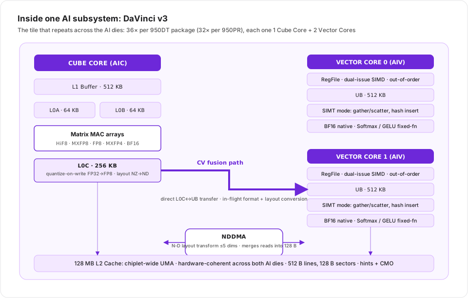
One AI subsystem of DaVinci v3: the tile repeats 36 times per 950DT package
The Cube Core: where the FLOPS live, and where the bits shrink
The Cube Core is the tensor engine, and v3’s headline is a new precision ladder:
| Format | 950DT peak (full config) | Relative |
|---|---|---|
| TF32 | 273 TFLOPS | 0.5× |
| BF16 / FP16 | 547 TFLOPS | 1× |
| FP8 / MXFP8 / HiF8 | 1,034 TFLOPS | 2× |
| INT8 | 1,034 TOPS | 2× |
| MXFP4 | 2,007 TFLOPS | 4× |
Two details matter more than the peak numbers:
On-the-fly quantization at L0C write-back. The 256 KB L0C accumulator buffer doesn’t just hold FP32 accumulation results: it converts them on the way out to BF16/FP16/FP8/INT8, and re-lays them out (NZ→ND) in the same operation. If your next consumer wants FP8, the 32-bit intermediate never pays DRAM bandwidth for being 32-bit. This is exactly the “fused online quantization in hardware” that DeepSeek-V3’s training report explicitly asked chip designers for (§3.5) after training a 671B MoE in FP8. Huawei read the same literature.
Bigger L0C for FlashAttention. A 256 KB accumulator supports more aggressive tiling of attention kernels, and Huawei claims 1.5–2× single-core FlashAttention performance over the previous generation via the fused Cube-Vector path (next section).
The Vector Core: fixed the bottleneck the last generation created
Previous Ascends had a dirty secret: the Vector Cores were weak enough that non-matrix work (Softmax, GELU, normalization: FlashAttention’s back half) starved the Cube Cores. v3 fixes it with a redesign:
- Register-based, dual-issue, out-of-order SIMD: a real vector machine now, not a vector coprocessor, with a RegFile between the Unified Buffer and the ALUs
- FP16/FP32 per-core throughput up 100%, plus native BF16 and a full set of conversion instructions
- Microcoded hot functions: Softmax and GELU get dedicated datapath treatment to keep the tensor ALUs fed
SIMD + SIMT on the same core
The genuinely novel bit is the programming model Huawei calls “new homogeneous” SIMD/SIMT hybrid. Each unit of work (a Vector Function) can run in either mode:
- SIMD mode (the default): regular element-wise work, dual-issue, high throughput
- SIMT mode (the escape hatch): irregular access patterns (gather/scatter, hash inserts, branching) get per-thread addressing like a GPU, without giving up the SIMD path for everything else
NVIDIA’s bet is SIMT with tensor cores bolted on; DaVinci’s is SIMD-first with a SIMT lane for the awkward 10%. Neither is wrong; they optimize for different distributions of work. For recommendation systems and multimodal preprocessing (real Huawei workloads), the SIMD-first split is defensible.
NDDMA and painless plumbing
Two quieter changes cut the cost of writing kernels: NDDMA, a DMA engine that performs up to 5-dimensional layout transforms (NCHW↔NHWC-style rearrangements, transposes) in flight while coalescing small reads into 128-byte sectors; and a BufferID synchronization mechanism that replaces Ascend’s famously fiddly set_flag/wait_flag discipline with something that looks like a mutex (get_buf/rel_buf). Neither shows up on a datasheet. Both show up in developer productivity, which is where Ascend’s real deficit has always been.
HiF8: an 8-bit float with (almost) FP16’s range
The most technically interesting part of the launch is a data format. Huawei published an academic version (“Ascend HiFloat8 Format for Deep Learning”, 2024), and the white paper confirms it’s native in the 950’s Cube Cores.
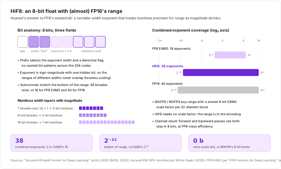
HiF8 trades mantissa precision for range as magnitude shrinks: a tapered, cone-shaped encoding
The problem with FP8 is that E4M3 spends its 8 bits badly for neural-network data: 18 powers of two of dynamic range, and out-of-range activations either saturate or need rescuing. The Microscaling formats (MX, now an industry standard) fix this by attaching a shared 8-bit scale factor to each 32-element block: that’s what MXFP8 and MXFP4 are. HiF8 makes a different trade: a variable-width exponent. A prefix code (“Dot”) declares how wide the exponent field is; the exponent is stored sign-magnitude with one hidden bit so the ranges of different widths never overlap; the mantissa gets whatever’s left. Precision is highest near |x| ≈ 1 and tapers off: 7 binades with 3 mantissa bits, 8 with 2, 16 with 1, per the paper. The result: 38 combined exponents (2⁻²² to 2¹⁵) versus E4M3’s 18, approaching FP16’s 40, in 8 bits, with no extra scale factor. Four special values (zero, NaN, ±Inf), no negative zero.
Why bother, when MX exists? Two reasons. First, the MX scale factor is real overhead: an extra 8 bits per 32 elements (25% overhead on FP4 storage), a second operand in every GEMM, and a whole microarchitecture of scale-handling. HiF8 needs none of it. Second, range: Huawei’s claim, supported by the paper’s simulations, is that HiF8’s dynamic range is wide enough to keep both forward and backward passes in 8-bit tensors, where E4M3-based recipes need 16-bit elsewhere in the step. That’s the same insight behind Intel’s trillion-token FP8 work (arXiv:2409.12517): the failures at scale are range failures. If the claim holds in production training, HiF8 is a genuinely elegant piece of engineering, and it says something that the format exists because one company controls the whole stack, format to compiler to silicon.
The package: two AI dies, two IO dies, and memory that doesn’t exist anywhere else
The Ascend 950 is not one die. It’s a chiplet assembly: 2 AI Dies + 2 IO Dies + 8 (950PR) or 4 (950DT) on-package memory stacks, joined by Huawei’s Clink die-to-die links and memory interfaces into a single UMA: one address space, hardware-coherent L2 across both AI dies, software none the wiser.
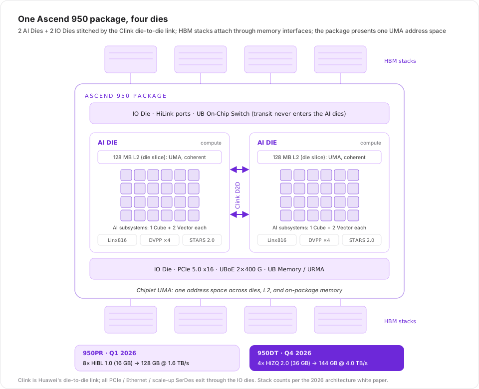
Ascend 950 package topology: the IO dies hold every SerDes, so scale-up transit traffic never touches the compute dies
The two-SKU split is the package used as a product strategy:
| Ascend 950PR (Q1 2026) | Ascend 950DT (Q4 2026) | |
|---|---|---|
| Role | Prefill & Recommendation | Decode & Training |
| AI subsystems (Cube + 2×Vector) | 32 (bin: 28) | 36 (bin: 32, 28) |
| MXFP4 / FP8 peak | 1,784 / 919 TFLOPS | 2,007 / 1,034 TFLOPS |
| On-package memory | 128 GB HiBL 1.0 @ 1.6 TB/s (bin: 112 GB @ 1.4) | 144 GB HiZQ 2.0 @ 4.0 TB/s (bin: 96 GB) |
| L2 cache | 128 MB (bin: 112) | 128 MB |
| AI CPU | Linx816, up to 8C16T | Linx816, up to 8C16T |
| UB interconnect | 2.0 TB/s bidirectional | 2.0 TB/s bidirectional |
(All full-config numbers from the white paper; the bins are the same silicon with redundant blocks disabled, since binning isn’t optional on a SAQP process.)
Why chiplets? The same reason everyone else does them: yield, amplified by the process. On N+3’s multi-patterned metal layers, a big monolithic die would be a yield catastrophe. Small AI dies plus relaxed-node IO dies plus binned SKUs is how you get a large chip out of a difficult node. NVIDIA does chiplets for HBM capacity and modularity; Huawei does them for survival, and the survival version looks structurally similar.
The IO dies are the quietly clever part. All 72 HiLink SerDes lanes (grouped as 18 ×4 ports at up to 112 Gbps), the PCIe 5.0 controller, and the two 400G Ethernet ports hang off the IO dies, and so does the UB On-Chip Switch. Transit traffic flowing through this chip to elsewhere in the rack gets forwarded on the IO die without touching a compute die or consuming DRAM bandwidth. It’s a switch built into the endpoint, and it’s the architectural foundation for the scaling story below.
Also worth naming: the memory. HiBL 1.0 (950PR) is Huawei’s self-developed, cost-optimized HBM: the keynote positioned it as cheaper than HBM3E; the shipped 950PR cards (Atlas 350, unveiled March 20, 2026) carry 112 GB of it, with teardown reporting of no Samsung, SK Hynix, or Micron content. HiZQ 2.0 (950DT) is the HBM4-class tier: 4 TB/s per chip. Reporting (Convequity, SemiAnalysis-adjacent) suggests the DRAM dies come from Swaysure with Huawei’s own base die (plausible, unconfirmed at fab level). Either way: the December 2024 HBM ban got answered in fourteen months, at volume, inside a shipping product.
The system bet: Unified Bus and the 8,192-chip SuperPoD
A chip two generations behind NVIDIA’s best cannot win alone. So Huawei changed the unit of competition (from chip to system), and Unified Bus (UB) 2.0 is the instrument.
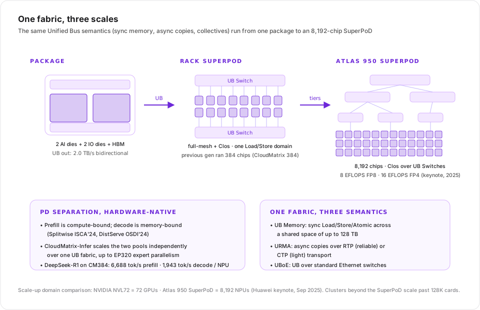
One UB fabric at three scales: the same memory semantics from package to SuperPoD
UB is a full interconnect stack, and its spec was publicly released in September 2025 with an open-source pledge attached:
- UB Memory: synchronous Load/Store/Atomic across a shared address space of up to 128 TB. Remote NPU memory behaves like local memory; there is no “copy then compute” step.
- URMA: asynchronous one-sided copies over queue pairs (“Jetties”), with two transport layers: RTP (end-to-end reliable retransmission, 4 ports) and CTP (lightweight, 9 ports).
- CCU: a Collective Communication Unit that hardware-executes Broadcast, ReduceScatter, AllGather, AllReduce and All2All off the compute cores, using its own memory slice and reduce units. Collectives stop stealing AI cores and NoC bandwidth.
- UBoE: UB tunneled over standard Ethernet, so a Huawei cluster can hop onto any existing datacenter fabric without new switches.
- Latency: 2.1 μs across the fabric, per the keynote; not NVLink-class, but the claim is that memory semantics (no copy, no handoff) beat raw latency at system scale.
The scale targets are where this stops being incremental. The previous generation’s CloudMatrix 384 already networked 384 chips; the Atlas 950 SuperPoD networks 8,192 of them: 160 cabinets, ~1,000 m², all-optical, 1,152 TB of on-package memory, 16.3 PB/s of aggregate interconnect, 8 EFLOPS FP8 / 16 EFLOPS FP4, targeted for Q4 2026. Huawei’s own comparison: 62× the interconnect bandwidth and 15× the memory of an NVIDIA NVL144 domain shipping the same period. Scale it again and the Atlas 950 SuperCluster crosses 520,000 chips at a zettaflop of FP4.
Is “weaker chip, vastly bigger fabric” a legitimate strategy? It’s arithmetic. If your chip is ~2× behind in FP8 and ~2.5× behind in memory bandwidth per chip, but you can network 8,192 of them with coherent memory semantics while your competitor’s scale-up domain is 72–144 GPUs, the system-level gap closes and partly inverts, at the price of floor space, optics, power, and software complexity. NVIDIA knows this; NVL144 and its roadmap are the same logic with better per-chip economics. The difference is that Huawei must win at this game, and so built UB (72 lanes per chip, port-multiplexed across scale-up, PCIe, and Ethernet) as a first-class citizen rather than a proprietary garnish.
Memory: the whole ladder, and the wall it’s aimed at
Put the whole hierarchy side by side and the design intent is legible:
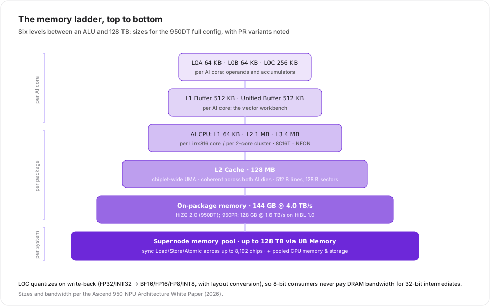
Six levels from ALU to 128 TB: note the on-package memory tier, which is where the HBM ban bit hardest
| Chip | Memory | Bandwidth | Per-chip FP8 | TDP |
|---|---|---|---|---|
| NVIDIA H20 (2024, legal China chip) | 96 GB HBM3 | 4.0 TB/s | 148 TFLOPS | 400 W |
| Ascend 950PR | 112–128 GB HiBL 1.0 | 1.4–1.6 TB/s | ~0.8–0.9 PFLOPS | ~600 W |
| Ascend 950DT | 144 GB HiZQ 2.0 | 4.0 TB/s | ~1.0 PFLOPS | n/a |
| NVIDIA B200 (2025) | 192 GB HBM3e | 8.0 TB/s | 4.5 PFLOPS (dense) | 1,000 W |
The L2 cache deserves its own note, because it’s where Huawei spent transistor budget that a TSMC node would have spent elsewhere: 128 MB, chiplet-wide, coherent across dies, 512-byte lines split into four 128-byte sectors, per-way locking, and programmable cache hints (a producer task can mark its output non-allocate so streaming junk never evicts the KV-cache-adjacent data the next task needs). Huawei claims 2× the previous generation on random and small-packet access patterns at equal bandwidth; for inference serving, where L2 hits on KV data are money, that’s a real number.
Per-chip against NVIDIA, the gap is what it is: roughly 4–4.5× behind B200 in FP8, ~2× behind in bandwidth, ~1.5× behind in capacity per chip. But note what the ladder does deliver: 144 GB and 4 TB/s is far past the H20 that served China for two years, and it exists at all only because Huawei was forced to build memory. The wall the ladder is aimed at is the KV cache, and there, capacity per system (1,152 TB per SuperPoD, plus pooled CPU memory over UB) is the metric that matters, not per-chip bandwidth.
What it means for how inference gets built: PD separation as silicon
The 950’s two SKUs (Prefill & Recommendation, Decode & Training) are a hardware encoding of an idea the systems community has been converging on for three years: prefill and decode are different workloads and should run on different machines. Prefill (processing the prompt) is compute-bound; decode (generating tokens) is memory-bandwidth-bound. Splitwise (ISCA ‘24) showed 1.4× throughput at 20% lower cost from splitting them; DistServe (OSDI ‘24) formalized the goodput math; Mooncake (FAST ‘25) runs it in production for Kimi with a pooled KV cache.
Huawei’s CloudMatrix-Infer paper (June 2025) is the missing production-scale proof: a 384-NPU UB fabric where prefill, decode, and KV-cache pools scale independently, with expert parallelism up to EP320. On DeepSeek-R1 it sustains 6,688 prefill tokens/s and 1,943 decode tokens/s per NPU (modest per-chip, multiplied by 384). The 950 series turns that architecture into product: buy PR cards for your prefill fleet and DT cards for your decode fleet, wired into one UB memory domain, with STARS 2.0 scheduling compute and CCU handling the collectives.
This is also the honest frame for the DeepSeek order. 160,000 950DTs (the decode-and-training SKU) for a datacenter that will serve inference for a 1.6T-parameter open-weights model whose CANN port landed on day zero. Reporting (SemiAnalysis, via InfoQ) claims V4 and the 950DT were co-designed: the model’s decode stage shaped around HiZQ’s 4 TB/s. Whether or not that’s exactly right, the direction is real: the hardware-software co-evolution that made CUDA’s moat is being attempted, at enormous scale, from the other side.
The honest scorecard
Where Huawei is genuinely strong:
- System architecture. UB’s memory semantics, the IO-die transit switch, hardware collectives, and 8,192-chip coherent domains are a coherent answer to the “per-chip deficit” problem, arguably a year ahead of NVIDIA’s scale-up ambition in topology, if not in per-node efficiency.
- Vertical integration under duress. Process (SMIC N+3), memory (HiBL/HiZQ), interconnect (UB), compiler (CANN, operator coverage reported up from ~30% to 80–90% since 2024), and now format design (HiF8). No other sanctioned company has pulled this off.
- Product-market fit inside China. The 950PR shipped on schedule (Q1 2026); Huawei targets ~750,000 950-series units this year; ByteDance alone has reportedly booked half the production line. IDC counted 812,000 Ascend cards shipped in China in 2025. The demand exists and is prepaid.
Where the gaps are real:
- Per-chip efficiency. ~4× behind B200 in FP8 per chip, and power tells the same story: the shipped 950PR does ~1.56 PFLOPS FP4 at 600 W where B200 does 4.5 PFLOPS FP4 (dense) at 1,000 W. N+3 costs you performance per watt, and no amount of chiplet trickery hides that.
- MFU and software gravity. The best published training run on Ascend hardware (a 1.6T-parameter post-training on ~1,000 910Cs) achieved 34.9% MFU against 50–55% typical on NVIDIA. CANN has closed most of the operator gap but not the ecosystem gap: CUDA is a decade of Stack Overflow answers, and every PyTorch workflow defaults to it.
- Yield and supply. SAQP yields are the industry’s known unknown; 2026 production (“low hundreds of thousands” of 950DT-capable output against a 750,000-unit target and a 4.2M-chip domestic demand estimate) means allocation, not purchase, is the bottleneck. DeepSeek needed Beijing’s help to jump the queue.
- Training, still. The 160,000-chip DeepSeek order is for inference. The training fleet remains NVIDIA (H800s) plus whatever Ascends can be spared. The 950DT is designed for training; nobody has demonstrated frontier-class pretraining on it yet. That proof point is the whole game, and it hasn’t been played.
The fair summary is not “Huawei caught NVIDIA.” It’s that Huawei removed NVIDIA’s leverage: for the workloads that dominate Chinese AI spend today (serving large open models at extreme scale), the domestic stack is now sufficient, cheaper per token, and immune to export policy. Compelling hardware everywhere was never the requirement.
What it means for the rest of the world
Three things, in ascending order of importance.
First, export controls changed the optimization problem instead of ending it. Cut off from EUV, China’s answer was DUV multi-patterning plus chiplets plus system-scale compensation: a worse chip and, for large-model serving, a competitive system. Cut off from HBM, Huawei built memory. Every restriction so far has been answered inside roughly eighteen months, at shipping volume. The controls still hurt (the power and yield gaps are permanent tax), but “deny” and “delay” are turning out to be different words.
Second, the unit of competition has moved from chip to system, and the interconnect won. NVIDIA’s NVLink, Google’s ICI, and now Huawei’s UB are the same admission: memory-bandwidth economics at cluster scale beat single-chip FLOPS. Watch UB specifically: it has published specs, an open-source pledge, and Ethernet interoperability (UBoE). Interconnect standards are how regional platforms go global; PCIe got there, InfiniBand got there, and a UB that works over any Ethernet switch is not a crazy candidate.
Third, the low-precision end is now a three-way format race. NVIDIA ships MXFP4/FP8, Huawei ships MXFP4/FP8 plus HiF8, and the research literature (MX, FP4 training, trillion-token FP8) has made sub-8-bit training respectable. Whoever’s tensor cores most natively express what the models actually need (block scaling, wide dynamic range, in-flight quantization) wins efficiency per dollar for the next generation. The Ascend 950’s format roster is a shot across that bow from a company nobody had on their format-race bingo card.
The scoreboard to watch for the rest of 2026: does the 950DT actually ship at volume in Q4? Does anyone publish frontier-class pretraining results on it? Does CANN’s open-source deadline hold? And when the Ascend 960 lands next year with 288 GB and 9.6 TB/s per chip, the question stops being “can China build an AI chip?” and becomes “how much of the world’s inference can it serve?”, which is a very different question, with a much larger answer.
Sources
Primary (Huawei):
- Ascend 950 NPU Architecture White Paper (2026): chiplet topology, DaVinci v3, HiF8, UB 2.0, STARS 2.0, CCU, memory hierarchy
- Eric Xu keynote, Huawei Connect (Sep 18, 2025): roadmap, HiBL/HiZQ, Atlas 950/960 SuperPoD and SuperCluster figures
- Ascend HiFloat8 Format for Deep Learning (arXiv:2409.16626)
- Serving LLMs on Huawei CloudMatrix384 (arXiv:2506.12708)
Teardowns and analysis:
- SemiAnalysis, “Is SMIC N+3’s Metal Pitch Smaller than Intel 18A’s?” (Jun 2026): all N+3 quantitative figures
- TechInsights, “SMIC N+3 Confirmed: Kirin 9030” (Dec 2025) and process-flow analysis (Aug 2026)
- SemiAnalysis, “Huawei AI CloudMatrix 384” (Oct 2025)
- Tom’s Hardware, Ascend roadmap and UB deep-dives (2025)
News:
- Bloomberg, “DeepSeek Plans Big Huawei AI Chip Order” (Sep 4, 2026)
- Reuters: DeepSeek V4 on Huawei chips (Apr 2026), US clears H200 for ten Chinese firms (May 2026)
- TrendForce: Atlas 350 debut (Mar 2026), 950DT pull-forward (Jun 2026)
Academic context:
- FP8 formats: arXiv:2209.05433 · Microscaling: arXiv:2310.10537 · DeepSeek-V3: arXiv:2412.19437 · FP4 training: arXiv:2502.20586 · Trillion-token FP8: arXiv:2409.12517
- PD separation: Splitwise, DistServe, Mooncake · Roofline survey: arXiv:2402.16363
Corrections welcome: figures marked as analyst claims are attributed, and the white paper remains the authority for everything on-chip.